Monday, December 13, 2010


The articles I read - 1: Xcell Journals from Xilinx


I read my first XCell Journal in 1996 when I started working with XC4000 family of devices. It is a wonderful archive of tips on FPGA/CPLD devices. All the past issues since 1988 are archived online here.
http://www.xilinx.com/publications/xcellonline/ 

Click on "Past Issues" tab to access old issues. Let me know if you find any interesting read.

Monday, November 8, 2010


Interview Question 10: Trouble-Free Switching Between Clocks

How do you gracefully switch between 2 asynchronous clocks?

Here is an answer from http://www.xilinx.com/publications/archives/xcell/Xcell24.pdf

Asynchronously selecting between two clock sources can easily produce glitches that cause unreliable system behavior. The circuit diagrammed here avoids these problems.


While the SELECT input is stable (either High or Low), the two control flip-flops are in opposite states and one of the two clock inputs drives the clock output. When the SELECT input changes, there is no immediate impact until after the next falling edge of the originally-selected clock source, which also resets its control flip-flop. The Output Clock signal will then stay Low until the next falling edge of the newly-selected clock. This edge will set its control flip-flop, causing this clock to drive the Output Clock. Thus, with this circuit, any switching between clock sources is delayed by holding the output Low from the time the first clock goes Low until the time the second clock is Low.


Monday, October 4, 2010


Interview Question 9: Logic to find out number of data chunks


In one of my past back-plane design I implemented a store and forward logic. The packet data was sent in chunks of 64 bytes. One chunks consisted of 62 byte of payload and 2 bytes of data which contained other useful information like pointers to other chunks, actual payload bytes in that chunk, and QOS related tags.

Can you design a smallest logic to find out the number of chunks needed for supplied packet payload?

Monday, August 9, 2010


Interview Question 8: Sneaking CPU read/writes when continuous Memory Read Writes are going on


With the advent of increased performance needs new design challenges arise. This questions deals with one of such problem. A single port memory is continuously accessed by surrounding data plane blocks. They are accessing memory in continuous fashion. For example W-R-W-R.... There is no empty clock cycle to waste. 

The software wants to access this memory through CPU read/writes intermittently. Usually a simple mechanism using a state machine can be used to sneak in CPU access when no data plane access is going on. The problem arises when when this request gets timed out as every clock is being used by data planes accesses. How does one resolve this problem?

Changing single port memory to dual port memory seems to be easy solution but what if it is prohibitively expensive and not allowed. As design geometries are also stretched to the limit, increasing/doubling clock rate of memory is also ruled out.

How will you approach this practical problem?

Monday, June 7, 2010


Interview Question 7: Enhance the memory

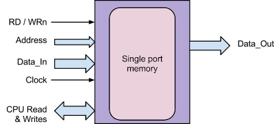
You are given a one port memory block as shown below.


In past you used this memory to design an application where you performed one read or write operation every clock. Now in next generation product you are asked to double the performance. How will you accomplish it? Brainstorm multiple scenarios.
For example:


1. How will you modify the design if you could double the clock at which memory can run?


2. What if you can not double the clock speed? How will you modify the design if you are asked to use memory at the same clock period as the surrounding logic.


I know, it is difficult to take out juice from the memory like this. What if you are asked just to allow (WRx + RDy) or (RD0 + RD1) combinations only? You may also use more than one memory to solve this problem.

Monday, March 8, 2010


Interview Question 6: 7 bit 1’s counter using 1 bit adders.

You are given a basic 1 bit adder block as shown below. 


How can you use this building block to create a module which finds out number of 1s in a 7 bit input?

Sunday, January 3, 2010


Interview Question 5: Design / Architect a solution

Design a solution (state machine, timing diagrams etc) for following problem.


Followup question: What are the possible error conditions. How to  find and recover from them?